This (not complete) list of processes available in our photovoltaics division reflects besides process equipment particularly those process steps used to manufacture solar cells and optimize the steps as well as the machines used therefore. Knowledge of physical parameters and properties of semiconductor materials and solar cells gained in this manner helps for the development of new concepts and technologies.
Wet chemical treatment
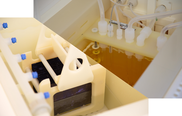
At the beginning of every crystalline silicon solar cell stands a raw silicon disc – a so called wafer. The wafer has to be etched and cleaned before further processing. These steps are carried out in different baths of the wet bench in our clean room.
Wet chemical texturization
The type of texturing depends highly on the crystal orientation of the wafers. While multi-crystalline wafers are usually acidic etched (‘acidic texture’ solution), mono-crystalline wafers are etched using an alkaline solution.
Alkaline texture
Alkaline texture consists mainly of KOH and a long-chained alcohol in solution. The resulting surface structure, formed in few minutes in the etch bath, of inverse pyramids in the micron range serves as a reduction mechanism for surface reflection of incoming light.
Acidic texture
Consisting of HF (hydroflouric acid), HNO3 (nitric acid) and H2O (deionized water), the solution was developed, patented and successfully licensed by University of Konstanz. The solution can be used for vertical (‘batch’) or horizontal (industrial, ‘in-line’) processing and etches only a few microns from the surface to form a worm-like structure to reduce reflection.
General cleaning processes
Next to standard industrial cleaning steps involving solutions of diluted HCl (hydrochloric acid) and HF, for highly pure processes involving high-efficiency solar cells cleaning processes like piranha clean (H2O2/H2SO4) or RCA clean (two-step process with H2O2/NH3 and H2O2/HCl) are used. Thereby, the choice depends on the application, objective and targeted costs.
Doped layer formation (e.g., emitter diffusion)
To form a doped layer using diffusion, the common process in industry is gas phase diffusion in a tube furnace. Thereby, doped glasses (boron silicate glass BSG or phosphorous silicate glass PSG) are grown directly on the wafer and the dopants diffuse into the wafer during this high temperature step.
Alternatively, doped glasses can be deposited before the high temperature step using CVD processes (see below). We focus on and drive especially this alternative process forward, which displays versatile and unique advantages including masking, structuring properties and the capability for co-diffusion of differently doped layers.
Nevertheless, by masking selectively parts of homogeneously diffused doped layers from gas phase diffusion (e.g., using etch resist materials printed by inkjet systems) and subsequently selective etching (emitter etch back EEB) in a nitric oxide containing solution of HF, HNO3 and H2O, the resulting wafer surface can be selectively doped, i.e., displaying different doping concentrations. This process was developed, patented and successfully licensed by University of Konstanz as well.
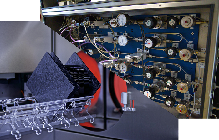
Deposition of dielectrics (e.g., CVD processes)
Deposition of dielectrics is carried out primarily using plasma enhanced chemical vapor deposition (PECVD) tools. Lighting a plasma in the process gas cloud in the low pressure system leads to dissociation of the gas molecules to form radicals for deposition of the dielectric film on the wafer surface. Thereby, the commonly known silicon nitride (SiNx:H) as well as silicon oxide in undoped (SiOx:H) or doped (BSG und PSG) form, amorphous silicon (a-Si) or other silicon based glasses can be deposited. Furthermore, by application of special tools, alumina (Al2O3 i.e., AlOx) can be deposited on the silicon substrate using atomic layer deposition (ALD) or atmospheric pressure CVD (APCVD). Dielectrics are utilized as anti-reflective coating, passivation layers, masking or barrier films, as well as for special applications depending on the solar cell concept. In some cases they can be used as multi-functional layers using more than one of these properties at once.
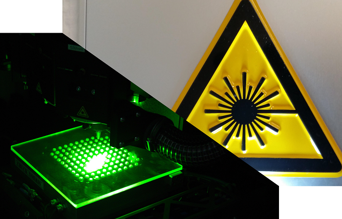
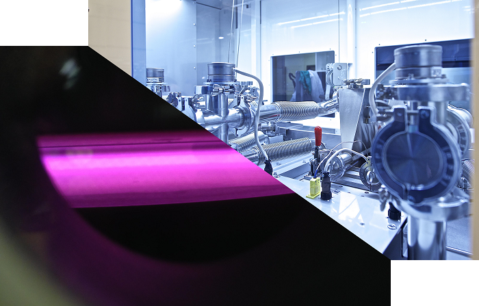
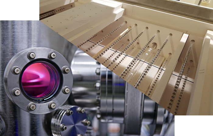
Laser processing
Lasers are increasingly applied as a versatile processing alternative to reduce process step number and duration. We use two nanosecond laser systems with three different wavelengths to cut, mark, laser-dope and ablate wafers and dielectric layers, respectively. Especially in case of ablation of dielectric films e.g., to open up layers before metallization (PERC cell design) we further utilize a picosecond laser system equipped with three wavelengths. The laser systems are semi-automatic to reflect both the throughput as well as the relevant aspects of automation in industry. Nevertheless, the high flexibility of different wavelengths, power range, as well as beam shaping allows also for physical fundamental research.
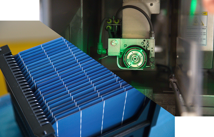
Metallization
To form the metal-semiconductor contact we use primarily common screen-printing, the technique common in industry. In this case, liquid metal paste is printed. Being the most common method to form this type of contact, it is still in further development towards optimization. Screen-printed cells are fired in a high temperature step in a belt furnace to form the contact, as well as to passivate crystal defects in the silicon bulk by hydrogen. In case of thermally sensitive cell concepts (e.g., hetero junction solar cells), high-efficiency cells or special test samples, we apply plating processes, that are partially in development, or common metal evaporation techniques (electron beam/thermal evaporation / sputtering). The latter methods work with impacting electron beams or high voltages on metal reservoir targets to evaporate metal particles and deposit them on the wafer in the vacuum chamber. In contrast to the necessary firing step involving screen-printing, the heat generation during plating or evaporation methods is lower. Therefore, the choice of metallization technique depends highly on the cell concept and the heat budget allowed.
RTP and annealing steps
To activate passivation films, carry-out hydrogen tests, sinter metallization or to perform tests on different materials for cell development under various high temperature conditions, rapid thermal processing (RTP) and annealing tube furnaces are used.
Special applications
Commonly, not only standard solar cells are manufactured, but also differently large, differently processed and samples covering a large parameter range are fabricated. Therefore, a semiconductor chip saw for edge and emitter layer isolation or a porosification tool to form porous silicon is used.