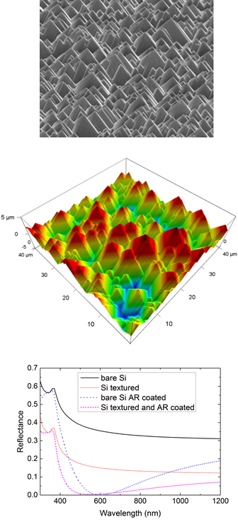
Closely connected to the PV industry our PV Division has many industrially focused research co-operations. In addition to these long term activities, in cooperation with the Steinbeis GmbH, we offer scientific services for short term needs. No matter if just a silicon sample has to be chemically cleaned, or if a complete batch of high efficiency cells with loss analysis is needed, after detailed advice, our specialists will prepare you an offer.

Here you find a short overview of available services and measurement techniques:
- Solar cell processing. Options include selective emitters, passivated rear sides and photolithographic contacts
- Partial processing of cells
- PECVD and ALD depositions, also with doped layers
- Complete loss analysis of solar cells with I-V and SR measurement
- Raman measurements
- AFM measurements
- Reflectance measurements
- Minority carrier lifetime measurements (temperature dependent and spatially resolved)
- Degradation measurements (LID)
- 4-point and ECV measurements
- TLM and CoRRe-scan measurements
- Ellipsometry and FTIR measurements
- Electro and photoluminescence measurements
- Lock-in thermography (iLIT, dLIT) measurements
- LBIC and EBIC measurements
- Electron microscopy (SEM) with focused ion beam (FIB), element specific analysis (EDX) and electron backscattering (EBSD)
- Optical emission spectroscopy with inductively coupled plasma (ICP-OES)
- Sputtering and evaporation of thin layers
- Chip saw for silicon and glass substrates
- Laser cutting and marking of silicon wafers
Further explanations of the characterisation methods can be found on the page of our characterisation group (Group Characterization) and here (Characterization). Some processing steps are explained at (Processing).
This group is also responsible for the abundant IT infrastructure of the photovoltaics division. To share data and knowledge we host our own file server and a private wiki.
