Motivation
With wafer costs of approx. 30-40% of the module costs, the Si wafer as the starting product for a solar module represents an important cost factor. Currently, more than 90% of all photovoltaic modules are manufactured on the basis of crystalline Si wafers, whereby different manufacturing techniques are used for these wafers. The resulting different defect distribution has a decisive effect on the subsequent solar cell efficiency. A good physical knowledge of the existing defects and their distribution, as well as a comprehensive understanding of their changes in the solar cell process can significantly improve the efficiency of solar cells for different Si material classes. Furthermore, it must be ensured that the remaining defects in the finished solar cell are in stable configurations in order to ensure stable operation of the solar module.
Si Wafer Materials
The quality of Si wafers has a wide range, with the quality of the Si feedstock used for crystallization already varying. Another factor is the type of crystallization: In the case of ribbon Si materials, the wafer is obtained directly from the Si melt, which makes complex sawing processes with the associated high material losses unnecessary and thus brings with it a decisive potential cost and energy advantage. However, these ribbon Si materials are subject to a high defect density due to the relatively rapid crystallization, which limits the potential of the solar cells produced from them.
In the class of block-cast multicrystalline (mc) Si materials, on which this group is currently having one of its foci, decisive improvements in crystallization have been achieved in recent years. Improved crucibles and crucible coatings reduce the diffusion of contamination into the Si ingot, which increases the usable material yield of a mc-Si block. The use of seed materials on the crucible base enables the crystallization of so-called quasi-mono Si, i.e. an almost monocrystalline Si material. In the case of the so-called high performance mc-Si, however, grain boundaries are still present, although the crystallization conditions have been optimized to the effect that this material for mc-Si has very long lifetime of the minority charge carriers of more than 1 ms in some cases. Nevertheless, block-cast Si wafers are subject to quality fluctuations due to their position in the mc-Si block, such as the dependence of the metallic impurity distribution over the block height or the density of dislocations.
In addition to the block-cast Si materials, various single-crystalline Si materials such as Cz- or FZ-Si with a significantly lower defect concentration are also used in this group. Some of these materials are considerably more complex to produce than mc-Si, but have a higher efficiency potential for solar cells. It is still unclear why mc-Si materials in locally monocrystalline areas usually do not reach the quality of single-crystalline Si materials, so that the continuous comparison of both material classes is carried out as standard in almost all experiments.
Si materials, which are too expensive for commercial PV applications due to their complex manufacturing process and high material purity, are used to investigate defect influences that are currently still covered by prevailing crystallographic or contamination-related effects in the materials used in the photovoltaic industry. These materials are of crucial scientific importance for understanding defects and the ultimate limitations of materials.
In addition to such high-quality materials, materials are used in this working group, particularly in the area of mc-Si materials, in which a type of defect, such as the concentration of one or more metallic impurities, is specifically increased and manipulated during crystallization. Such changes in material quality and properties simplify the investigation of the effects of individual defect types on the Si material quality and their changes during the solar cell manufacturing process.
A precise knowledge of the material properties of these different Si material classes is of decisive importance if the behaviour of defects in the solar cell is to be understood and the potential of these Si materials for photovoltaic applications is to be determined.
Defect Characterization
For the evaluation of the material quality a comprehensive characterization of the defects in the available Si materials is very important. Of particular importance here is the determination of the minority carrier lifetime, which is a measure of material quality and initially provides indirect indications of the underlying defects. Injection- and temperature-dependent lifetime measurements allow conclusions to be drawn about further defect properties. Spatially resolved lifetime measurements and their comparison with other measurement methods allow conclusions to be drawn about the underlying defect structure. The determination of the interstitial Fe concentration is also based on specific lifetime measurements.
The separation of volume and surface effects is decisive for lifetime measurements. A sufficiently good surface passivation is necessary in order to be able to make statements about the actual bulk lifetime of interest. However, a disadvantage of established processes for surface passivation is that the deposition of the passivation layers is usually associated with temperature steps or an entry of H into the volume, which can have effects on the electrical activity of the defects. For this purpose, these surface passivations are optimized for lifetime measurements and new wet-chemical processes are investigated that minimize or ideally do not exhibit these volume changes at all.
To correlate the lifetime with the underlying defect structure, further methods are used to determine crystallographic properties, such as the localization of grain boundaries, the determination of crystal orientation and dislocation density. Furthermore, microscopic methods are used to determine the local recombination activity of defects or to directly detect impurities, such as the analysis of TEM lamellae or the 3D FIB method developed in this working group for the detection of metallic precipitates.
Defect Evolution during Solar Cell Production
The defect structure in Si materials changes during the solar cell process. High-temperature processes, such as the gettering of impurities during emitter formation or the final firing for contacting and for driving in hydrogen, are usually decisive here. The effectiveness of such process steps depends very much on the type and distribution of defects. The exact interaction of the existing defect structure with applied process steps is the subject of current research. For this purpose, the samples are subjected to a detailed defect characterization after each individual (partial) process step or after application of only individual process parameters such as temperature.
The current focus of this working group is on the process steps of gettering, the influence of H-passivation and firing. With regard to the getter process, established methods such as POCl3 diffusion are compared with novel approaches of a doping glass deposited by APCVD and subsequent diffusion. In addition to understanding the interaction of these process steps with the defect structure, it is just as important to maintain or even improve the properties of these process steps, such as emitter formation, which are important for the electrical function of a solar cell.
The H-passivation of defects by firing a H-rich dielectric layer represents a further process step that has a strong effect especially on the electrical properties of defects. The firing step, which normally concludes the solar cell process, changes the defect properties once again due to the high temperature input and can also lead, for example, to already gettered impurities redistributing in the material. In addition to understanding the interaction of defects with individual process steps, it is therefore extremely important to always keep an eye on the entire solar cell process.
Long-term Stability
Various degradation mechanisms and the long-term stability of solar cells have developed into a hot research topic in recent years. Recombination-active boron-oxygen (BO) correlated defects form under charge carrier injection (e.g. under illumination) especially in monocrystalline Czochralski-Si and reduce the efficiency of the solar cell under working conditions. A very elegant way of reversing the harmful effects of this phenomenon, also known as light-induced degradation (LID), was discovered at the University of Konstanz in 2006. This process, known as regeneration, allows the harmful effect of BO-correlated defects to be completely eliminated after solar cell production. To this end, intensive research and development work has been and continues to be carried out.
The research group also deals with LeTID (Light and elevated Temperature Induced Degradation) in mc-Si and the subsequent regeneration under the same conditions. In addition to effective external gettering steps, the influence of the firing step is of central importance. To limit the underlying defect, the measuring conditions, such as temperature, are also varied. Based on these investigations, first model ideas of the underlying defect or the factors influencing this defect (hydrogen and metallic contaminations) could be found. However, the cause of LeTID and the exact defect evolution during degradation and subsequent regeneration is still far from conclusive.
LeTID occurs in all classes of mc-Si materials. The lifetime level at maximum degradation hardly differs between cost-efficiently manufactured or even deliberately contaminated materials compared to high-quality mc-Si materials with initial service lives of up to 1 ms. In the meantime, there are also indications that LeTID is not limited to mc-Si, but also occurs in monocrystalline materials.
Characterization of new Silicon Materials
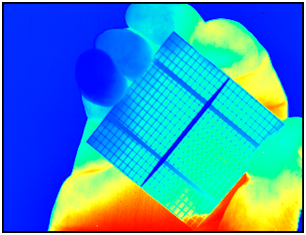
Within the scope of the available resources, fundamental research and investigations are carried out, such as studies of the crystal structure of the Si materials and the recombination properties of the crystal defects. Together with the Characterization group, measurement techniques are also being developed and used that are not yet available within the framework of existing projects and collaborations. For this purpose, e.g. measuring stations are set up, which can display the characteristics of the Si materials in a spatially resolved way. Examples of this are lock-in thermography, with which the smallest temperature changes down to the µK range can be detected on a solar cell and thus provide information about sources of loss within the solar cell, as well as time-resolved photoluminescence.
The picture shows a 5x5 cm2 solar cell held in the hand. It was recorded with an IR camera that is sensitive in the wavelength range 3-5 µm. Si is transparent in this wavelength range, since the photon energy there is smaller than the band gap energy of Si. Therefore, besides the front metallization, the backside metallization (grid structure with two busbars) can also be seen through the cell. In the color coded display, red areas are warmer and blue areas are colder.