The process technology group is working on the improvement of industrial manufacturing processes for mono- and multicrystalline silicon solar cells. For this purpose, new concepts and technologies are investigated and, if regarded as technically feasible and economically promising, developed to pilot line level in order to transfer them to industrial production with our partners. The pursued concepts are chosen by their short to medium term applicability and the potential of reducing the cost of photovoltaic electricity. This application-oriented work is supplemented by research activities that aim on a deeper understanding of the devices and individual process steps.

Selective Emitter (SE)
Reducing the front side losses of a solar cell can be accomplished by implementing a selective emitter. In this concept, only the metallized emitter region is heavily doped in order to ensure a low contact resistance, while the illuminated surface is weakly doped to reduce the recombination losses. A patented etch-back process for the production of selective emitter solar cells was developed in the industrial solar cells group which is currently being marketed by the equipment manufacturer Gebr. Schmid GmbH.

Passivated Rear Side
In order to reduce the recombination losses at the cell back side, the full area aluminum back-surface-field (BSF) of a standard solar cell can be replaced by a dielectric passivation. For contact formation this layer is firstly opened locally, e.g. by laser ablation or masked etching. Afterwards aluminum paste is screen-printed over the full rear surface. During the contact firing step, a local BSF is formed in afore opened areas, thus ensuring a field effect passivation of the highly recombination-active surface.
For surface passivation by aluminum oxide, an Oxford atomic layer deposition (ALD) tool is available. As an inexpensive alternative, the deposition by atmospheric pressure chemical vapor deposition (APCVD) is also subject of the current research activities in the industrial solar cells group.

n-Type Solar Cells
The minority charge carrier recombination in the base constitutes one of the main power losses of standard silicon solar cells. The successful optimization of the individual process steps in the recent years increases the share of the base recombination to the total losses, furthermore most future cell concepts require a higher quality of the base substrate. Up to now the vast majority of industrially manufactured solar cell uses p-type silicon which typically features a minority carrier lifetime of below 1 ms. Especially in boron doped Czochralski (Cz) silicon wafers recombination-active boron-oxygen complexes form under illumination which lead to light-induced degradation of the minority carrier lifetime.
Significantly higher minority carrier lifetimes can be achieved by using phosphorus-doped n-type Cz silicon which has a lower sensitivity for metallic impurities and is only marginally affected by light-induced degradation due to the very low boron content.
The so-called PHOSTOP cell concept is the easiest way produce a solar cell based on n-type silicon. The cell process widely corresponds to the standard p-type solar cell process. The front surface of the n-type base is passivated by a diffused phosphorus front surface field (FSF) while the alloyed aluminum profile creates the n/p junction on the rear side where the charge carriers are separated. The reduced recombination current in the base leads not only to an increase of the open circuit voltage but also the n-type base contributes to the lateral conductivity between the front contact fingers thus increasing the fill factor. In combination with an improved front side passivation, efficiencies of up to 19.5 % were achieved with this cell concept on large area Cz silicon at the University of Konstanz.
Bifacial Solar Cells
Bifacial solar cells have a passivated rear side which is contacted by a grid structure similar to the front side. Since only the contacted area is covered with metal, such a solar cell can absorb light from both sides. Presuming an adequate installation, up to 20% more electricity can be produced over the day. E.g. a vertical mounting with east-west orientation of the surfaces leads to a redistribution of power generation to the morning and afternoon. This can help to compensate the typical midday peak of PV electricity fed into the power grid.
Besides the passivation of the rear surface, a bifacial solar cell usually features a doping profile below with the inverse polarity of the front side doping. This improves not only the lateral conductivity but also reduces the contact resistance and contributes to the electric field effect passivation of the surface. Bifacial solar cells can be produced from p- or n-type silicon. Depending on the polarity of the base and surface doping, the emitter is located on the front or the rear side of the solar cell.
Current research activities of the industrial solar cells group on bifacial solar cells focus on the cost effective and desirably simultaneous generation of the doping profiles as well as the reduction of recombination and series resistance losses associated with contacting boron-doped surfaces.
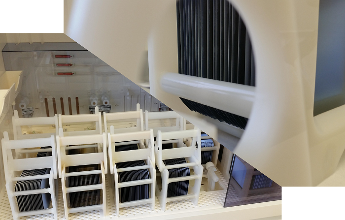
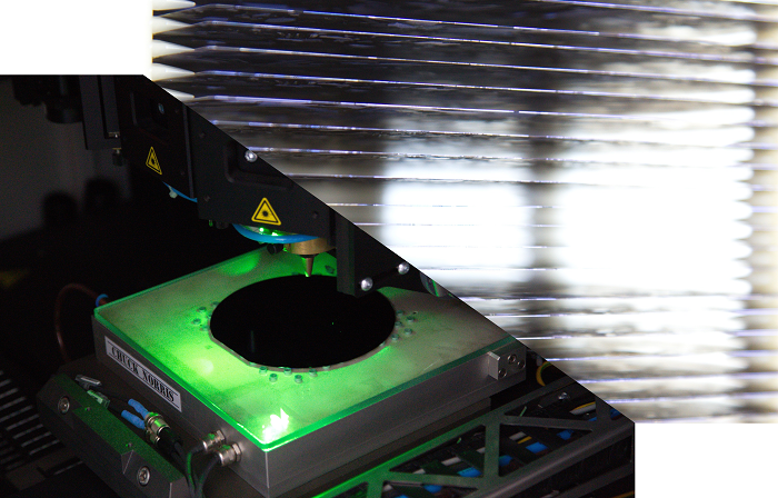
Solar cell processing takes place using industrial, prototypal or self-build large-scale machines. Being the core of the infrastructure, this equipment is used in a large variety to process the silicon material from the as-sawed wafer to the contact formation of the final solar cell. Thereby applied technology meets the highest requirements used in advanced photovoltaics sector. Processing of any type of solar cell includes a differently large number of process steps, which are used varyingly, but adapted after another depending on the type of silicon material or chosen solar cell design.
Cleaning and surface topography treatment
Any solar cell manufacturing process starts with the conditioning of the raw wafer. Depending on the starting quality, the type of material and the condition of the surface of the silicon wafer it is treated by a certain series of wet-chemical etching steps with the aim to rid the surface of the maximal possible or at least necessary amount of impurities (metal and organic compounds). The idea behind it, is to prevent the parasitic indiffusion of potentially defect-generating impurities into the silicon bulk during the following processing steps, e.g., the purposeful indiffusion of dopants by high-temperature treatment.
Beside the different cleaning steps with different chemical composition (e.g., HF/HCl solution; H2SO4/H2O2 solution; etc.) it is possible to direct-etch the silicon wafer surface to change the topography in a targeted way. This mechanism, known as texturization, is attained using either alkaline or acidic etch solutions resulting in a crystal-orientation dependent surface structuring of inverse pyramid or intertwined worm-like surface shapes, respectively. Changing the surface topography in such a way results in a decrease of reflection and increase in efficiency, yet requires qualitatively high-grade surface passivation due to the increased surface area.
Dopant-diffusion and surface passivation
Directly after cleaning the wafers are commonly doped by indiffusion of dopants in a tube diffusion furnace. Thereby, the used doping source for the high-temperature step can be grown in-situ from the gas phase or be pre-deposited by i.e., CVD. At the end of the diffusion step the pn-junction has been formed necessary for the separation of charge carriers within the silicon bulk. During the indiffusion of dopants gettering of impurities from the silicon bulk occurs, increasing the quality of the material. To maintain this clean state and to saturate the remaining open silicon bonds commonly a dielectric layer is deposited on the surfaces of the wafer. Using multi-purpose layers with additional properties, such as decreasing reflection, increasing passivation and supporting contact formation further increases the cell efficiency. These layers are primarily deposited using CVD reactors in which gases are transitioned into a plasma state to deposit these solids.
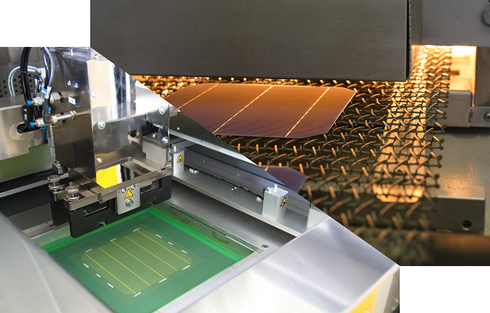
Metallization
The final step in solar cell processing constitutes the contact formation of differently doped areas on the wafer surface. Thereby, common and as industrial standard understood screen-print techniques as well as such being in development are applied. At the end a metal contact between semiconductor and in a module interconnectable material is realized. In case of metal screen-printing pastes, the contact formation to the silicon bulk is achieved in a throughput belt-furnace.
Technology
To display all these standard to highly experimental processing steps and sequences a corresponding supply infrastructure is necessary next to the large machine park. Especially in case of this local interconnection of fundamental research and industry-related processing for the development of solar cell concepts a comparable highly variable equipment operation considering possible parameters and flexibility to design new machine prototypes is necessary.
Process equipment
The machine park for processing solar cells consist mainly of large-scale machines, which are operated from manually to fully automated. Depending on the machine the throughput thereby ranges from a single wafer for research purposes to industrial scale of a few hundred wafers to depict real industry circumstances. Some machines include the following:
- Wet chemical process benches
- Tube diffusion furnace
- E-gun and sputtering equipment
- Nano and picosecond laser machine systems
- RTP and annealing ovens
- PECVD, ICP-PECVD, APCVD und ALD tools
- Screen-printing line (screen-printer and dryer)
- Belt firing furnace
- Inkjet system
- Chip saw
- Porosifying equipment
- Assorted large-scale characterization tools (ICP-OES, GD-OES, REM, etc.)
Additionally, the infrastructure includes the upkeep of the functionality of the machines, i.e., the maintenance and repair of the equipment, as well as the media supply (e.g., water, cooling water, deionized water, CDA, nitrogen, specialty gases, power and any other consumables). Special attention is given to working safety, especially in use of specialty gases in e.g., CVD reactors.